Survey on Pulsed Electrom Beam Deposition Work in
Technique and Medicine
C. Schultheiss, P. Brenner, L. Buth, and H. Bluhm
Forschungszentrum Karlsruhe GmbH,
Institute for Pulsed Power and Microwave Technology,
P.O. Box 3640, D-76021 Karlsruhe, Germany
The principal benefits of the PED (Pulsed Electron Deposition) coating method using Channel Spark are the simplicity of the system itself and the excellent coating results as for instance conservation of stoichiometry even in complicated alkali-earth alkali compounds within 1% to 2% and growth rates up to 1Ǻ per shot (see Fig.1). The coating process relies on ablative generated molten droplets of nano scale, which are deposited amorphous onto the surface of the substrate. Even plastic substrates and thin plastic foils can be coated provided the repetition rates are low enough. Since the initial capital- and operational costs are low in comparison with PLD (Pulsed Laser Deposition), there is a wide field of actual and future applications of PED which are summarized in this presentation. Actual efforts are the development of High-Tc-Superconductor cables, production of Nanotubes, organic LEDs and the coating of metallic or plastic medical implants with bioactive glasses. Other applications are the coating of plastic foils with 100 nm barrier layers to reduce the permeation of gases. Related tasks are the coating of ink cartridges made of plastic with a glass layer to prevent drying out. Another field of application is the ablation of PE, Polystyrene, PTFE etc. for coating surfaces. Besides optical effects of aesthetic value, PTFE coatings have a low molecular weight, are soft and can be used as extra thin sealants (thickness 40-100 µm) in chemical industry.
![]()
![]()
![]()
![]()
![]()
![]()
![]()
![]()
![]()
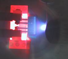
![]() Fig.1: Typical coating situation. The
photograph shows the ablation cloud (right), emerging from the target as well
as the substrate (left), which is externally heated.
Fig.1: Typical coating situation. The
photograph shows the ablation cloud (right), emerging from the target as well
as the substrate (left), which is externally heated.